STM32 #13: Finishing microSD initialisation and asking for its birthday
Last time I managed to get the STM32F103x talking to a microSD card over SPI. The card responded correctly to CMD0 and CMD8, which showed that the wiring, SPI mode, CMD packet format, dummy clocking, and R1/R7 response handling were functional. However I did not finish the initialisation process so let’s do that now. This post will finish the initialisation process and ask it for some information about itself!
Where we stopped:
- CMD0 response = 01 - Card entered idle state
- CMD8 response = 01 00 00 01 AA - Card accepted the voltage/check pattern command
The remaining sequence to complete initialisation is:
- CMD55 + ACMD41 repeatedly until R1 = 0x00
- CMD58 to read the OCR
- Check the CCS bit to detect SDHC/SDXC
- Increase the SPI speed (Optional)
After that, the card is ready for data token type reads. Before jumping into CMD17 (not in this post), I’m going to use CMD9 and CMD10 to read the CSD and CID registers.
CMD55 and ACMD41
ACMD41 is the command used to ask the SD card to finish initialising. It is an “application specific” command, so it is not sent by itself, you have to send CMD55 first, which tells the card an application specific command is coming next.
The sequence is:
- CMD55
- ACMD41
- Check R1 response
- Repeat until R1 = 0x00 (Ready, no error flag)
For SD v2 cards including SDHC and SDXC,ACMD41 should set the High Capacity Support (HCS) bit:
#define SD_ACMD41_HCS 0x40000000u
The HCS bit is not the card’s capacity, that is reported later with the CCS bit, this is just to tell the card that the host can support HCS.
I’m going to create some new macros to add to our existing code from the last post to make the code a bit more meaningful rather than having raw values in the main code block:
#define SD_CMD55 55u // Send application command
#define SD_ACMD41 41u // Initialise command
#define SD_CMD58 58u // Read OCR register

#define SD_DUMMY_CRC 0xFFu

#define SD_ACMD41_HCS 0x40000000u
#define SD_OCR_CCS 0x40000000u

#define SD_R1_READY_STATE 0x00u
#define SD_R1_VALID_MASK 0x80u

#define SD_BLOCK_SIZE 512u
#define SD_DATA_TOKEN 0xFEu

#define SD_ACMD41_ATTEMPTS 10000u
#define SD_DATA_TOKEN_ATTEMPTS 100000u
Tracking the card type
The driver needs to remember whether the card uses block or byte addressing. For SDHC and SDXC cards, the address passed to CMD17 is a 512 byte block number. For SDSC cards, the address needs to be a byte address. So we will make a card type enum:
typedef enum {
    SD_CARD_TYPE_UNKNOWN = 0,
    SD_CARD_TYPE_SDSC,
    SD_CARD_TYPE_SDHC_OR_SDXC,
} sd_card_type_t;

static sd_card_type_t sd_card_type = SD_CARD_TYPE_UNKNOWN;
Waiting for ACMD41 to complete
The next function to build will repeatedly send CMD55 + ACMD41 until the card leaves idle.
static sd_status_t sd_wait_ready_cmd55_acmd41(void) {
    uint8_t r1 = 0xFFu;

    for (uint32_t i=0; i<SD_ACMD41_ATTEMPTS; ++i) {
        sd_status_t status;

        // Send CMD55 - Prefix before application-specific command
        status = sd_send_command(SD_CMD55,
                                0x00000000u,
                                SD_DUMMY_CRC,
                                &r1,
                                NULL,
                                0u);
        if (status != SD_OK) { return status; }
        if ((r1 & SD_R1_ILLEGAL_COMMAND) != 0u) {
            return SD_ERR_UNSUPPORTED_CARD;
        }
        if ((r1 != SD_R1_IDLE_STATE) && (r1 != SD_R1_READY_STATE)) {
            return SD_ERR_BAD_RESPONSE;
        }

        // SEND ACMD41 - Application specific, Initialise card, with HCS bit set
        status = sd_send_command(SD_ACMD41,
                                 SD_ACMD41_HCS,
                                 SD_DUMMY_CRC,
                                 &r1,
                                 NULL,
                                 0u);
        if (status != SD_OK) { return status; }
        if (r1 == SD_R1_READY_STATE) { return SD_OK; }
        if (r1 != SD_R1_IDLE_STATE) { return SD_ERR_BAD_RESPONSE; }

    }

    return SD_ERR_TIMEOUT;
}
The loop treats SD_R1_IDLE_STATE as acceptable while the card is initialising. If the card returns SD_R1_READY_STATE the function returns SD_OK. If the card reports an illegal command it returns SD_ERR_UNSUPPORTED_CARD.
For the SDHC card I am using, ACMD41 should be supported, so an illegal command here would be a strong hint that something is wrong with the command sequence or the card is a different type.
The timeout values are arbitrary at this stage. It is there to stop the driver getting stuck if the card never leaves idle state.
Reading the OCR register with CMD58
Once ACMD41 completes successfully, the card should be ready. So now we will build a function to read the Operating Conditions Register (OCR).
In SPI mode, CMD58 should return an R3 response: R1 (1 byte) + OCR (4 bytes).
The sd_send_command() function already supports this because it can read an optional response tail after the first R1 byte. Let’s build the function:
static sd_status_t sd_cmd58_read_ocr(uint32_t *ocr) {
    if (ocr == NULL) { return SD_ERR_PARAM; }

    uint8_t r1 = 0xFFu;
    uint8_t r3_ocr[4];

    sd_status_t status = sd_send_command(SD_CMD58,
                                         0x00000000u,
                                         SD_DUMMY_CRC,
                                         &r1,
                                         r3_ocr,
                                         sizeof(r3_ocr));
    if (status != SD_OK) { return status; }
    if (r1 != SD_R1_READY_STATE) { return SD_ERR_BAD_RESPONSE; }

    // Split the OCR register into individual bytes
    *ocr = ((uint32_t)r3_ocr[0] << 24) |
           ((uint32_t)r3_ocr[1] << 16) |
           ((uint32_t)r3_ocr[2] << 8) |
           ((uint32_t)r3_ocr[3]);

    return SD_OK;
}
Like before the OCR bytes are returned most significant byte first, so the code rebuilds the 32 bit register by bit shifting left each into uhhh… the right position.
The Card Capacity Status (CCS) bit is key here, if it is set then the card is SDHC or SDXC and uses block addressing. If CCS is clear, then the card is an SDSC and uses byte addressing.
Updating sd_card_init()
Now we can finish the init function we started in the last post by adding the functions we have just built to the bottom of the init:
// CMD55 & ACMD41
    status = sd_wait_ready_cmd55_acmd41();
    if (status != SD_OK)  { return status; }

    // Read OCR CMD58
    uint32_t ocr = 0u;
    status = sd_cmd58_read_ocr(&ocr);
    if (status != SD_OK) { return status; }

    // Check CCS bit and set card type
    if ((ocr & SD_OCR_CCS) != 0u) {
        sd_card_type = SD_CARD_TYPE_SDHC_OR_SDXC;
    } else {
        sd_card_type = SD_CARD_TYPE_SDSC;
    }

    // Set SPI speed to fast
    spi_status = bsp_spi1_set_fast();
    if (spi_status != BSP_SPI_OK) { return SD_ERR_SPI; }
Testing the full sd_card_init() sequence
Now we can have a crack at running the full init and checking on the scope, if you don’t have a scope then you’ll need to write some UART logging to a terminal or something.
The first byte of each command packet has the form 01xxxxxx, where the lower six bits contain the command index. This is why CMD58 becomes 0x40 | 0x3A = 0x7A. For the logic analyser results to make sense we will create a conversion table for the commands:
| CMD | Unsigned Int | 6 bit hex conversion with prepend | Hex result |
|---|---|---|---|
| CMD0 | 0u | 0x40 | 0x00 | 0x40 |
| CMD8 | 8u | 0x40 | 0x08 | 0x48 |
| ACMD41 | 41u | 0x40 | 0x29 | 0x69 |
| CMD55 | 55u | 0x40 | 0x37 | 0x77 |
| CMD58 | 58u | 0x40 | 0x3A | 0x7A |
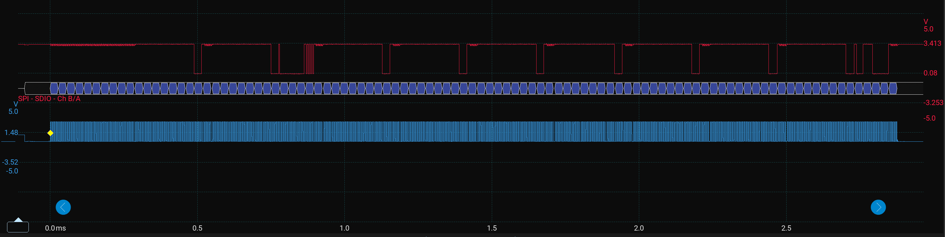
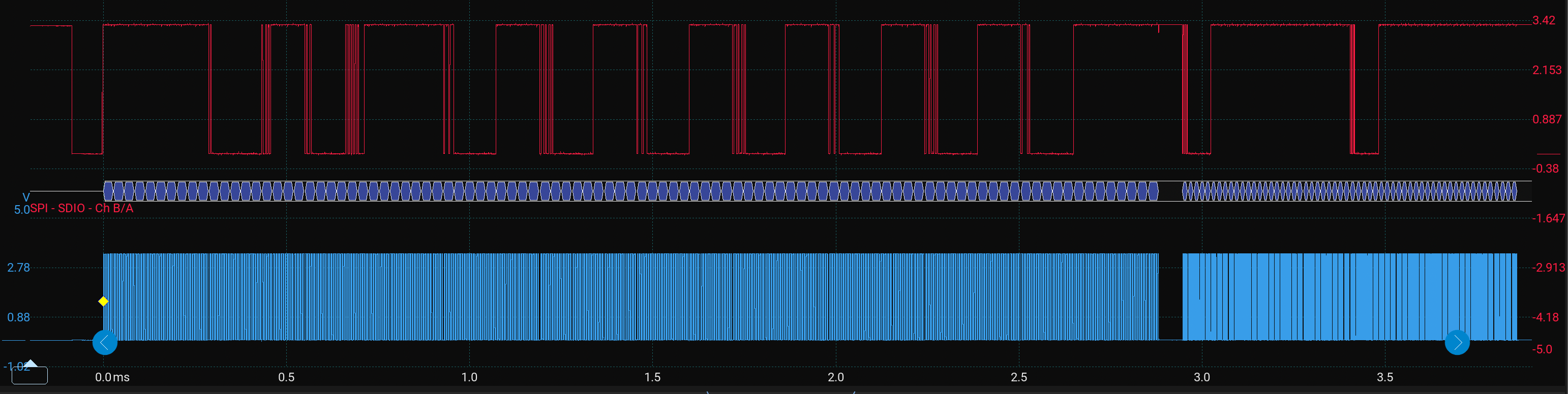
Let’s get a capture on the MOSI line first:
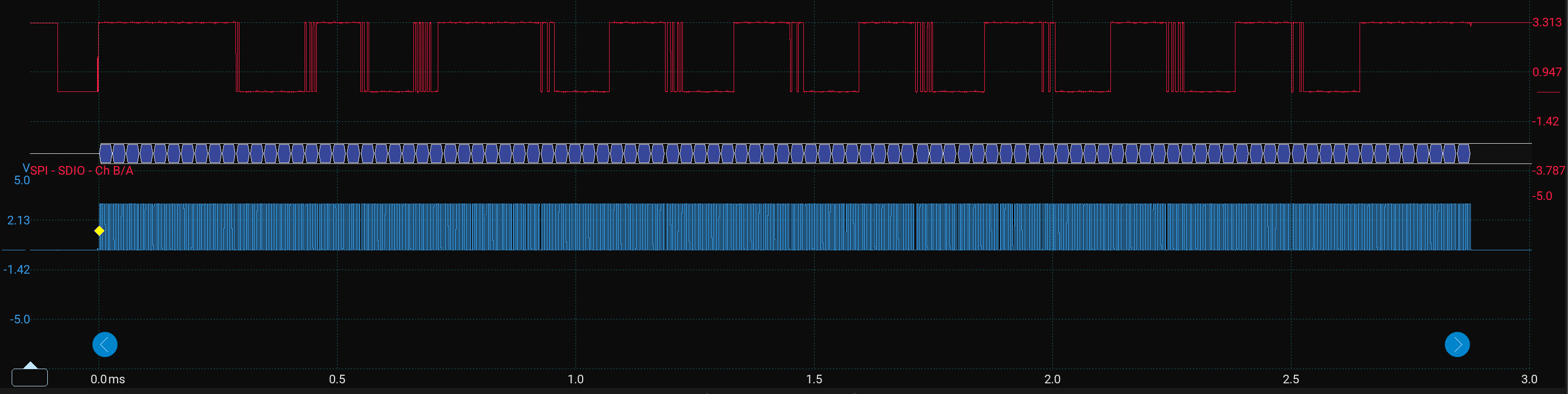
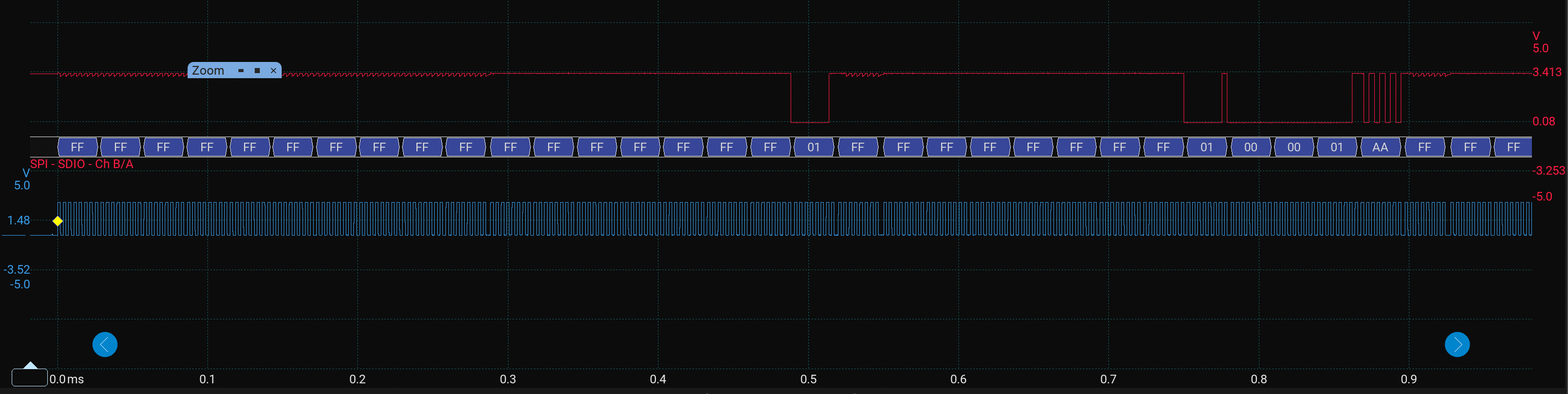
There is a lot going on there so let’s zoom in to the start:
Here we see the sequence we have covered in the last post so everything looks good so far, let’s move onto the next segment
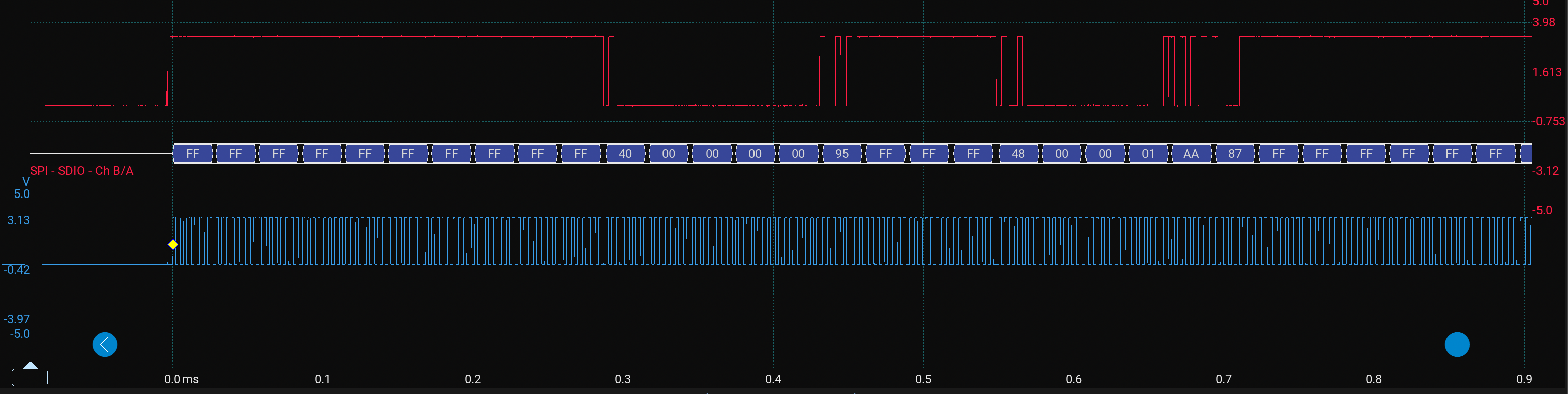
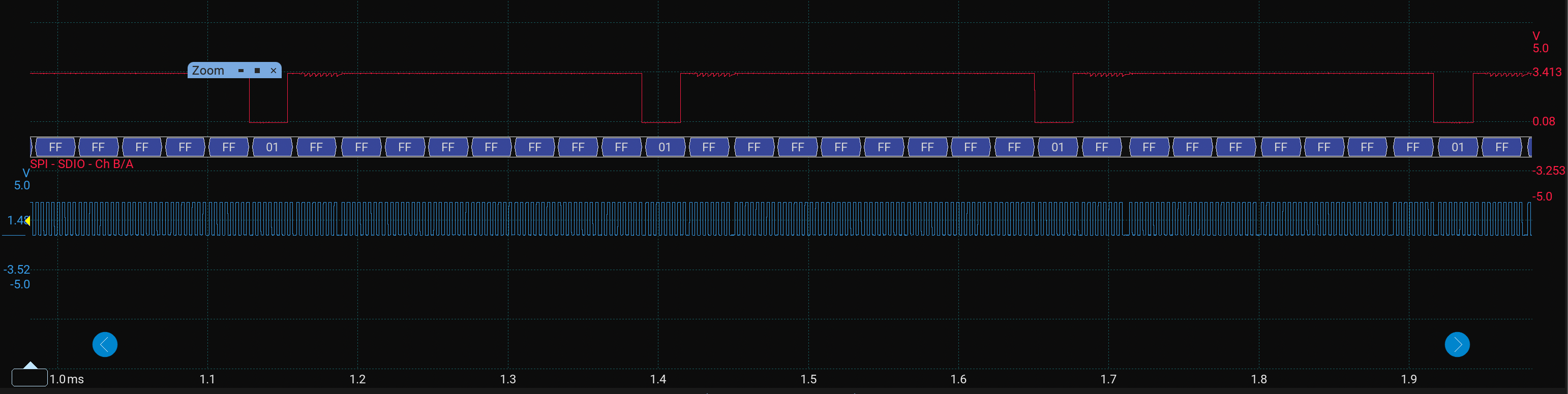
Brilliant, we can see the repeating sequence:
77 00 00 00 00 FF= CMD5569 40 00 00 00 FF= ACMD41
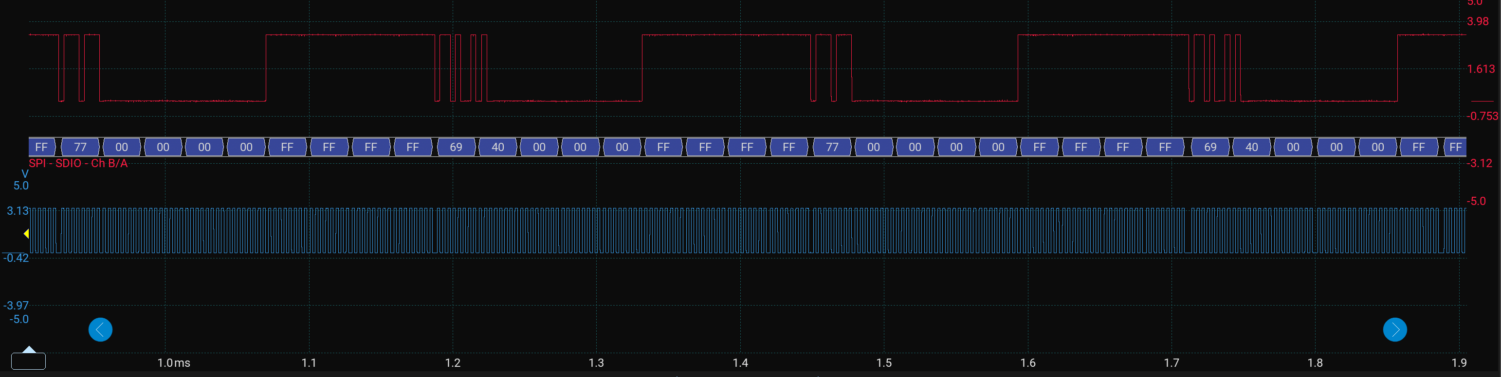
Then if we scroll forward we see:
We have another repeat of CMD55 + ACMD41, then we move onto:
7A 00 00 00 00 FF= CMD58
Brilliant so it looks like the last command in the init sequence was run on the MOSI, let’s check the responses on the MISO line:
Zooming into the first segment:
 Here we can see:
01= Response to CMD0 - Card Idle01 00 00 01 AA FF= Response to CMD8
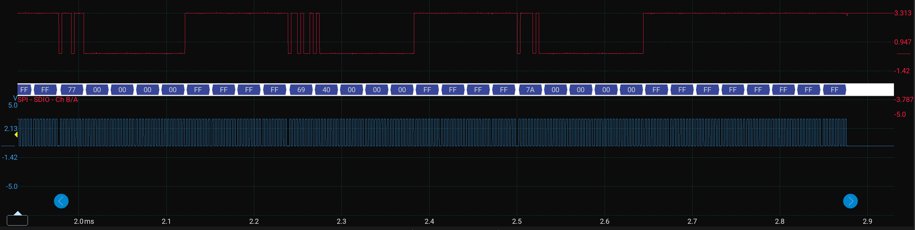
scrolling along:
01= Response to ACMD41 - Card still idle
Then finally we have:
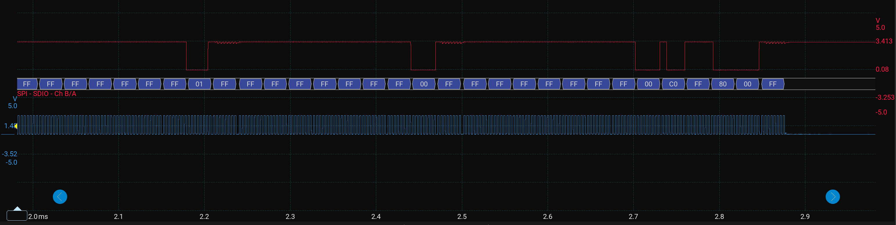
First we have another response to ACMD41. Then finally we see:
00= ACMD41 response - Card ready00 C0 FF 80 00= CMD58 response R1 + OCR value
Converting the 32 bit hex OCR value to binary we get: 11000000 11111111 10000000 00000000 The OCR is telling us:
- bit 31 = 1 Power up initialisation complete
- bit 30 = 1 which indicates the CCS is set so SDHC or SDXC.
- bit 29 = 0 UHS-II is not indicated
- bit 24 = 0 1.8v switching not accepted
- bit 23:15 = all 1s so the card supports the full 2.7-3.6v operating range
- bit 14:0 reserved
The initialisation appears to have been a success and we can account for all the results on the MISO line mostly (Confidence would be closer to 100% if I could have had the CS line on the logic analyser. Alas, I must work with 2 probes for now.)
Let’s have a chat with the card
There are some other commands you can use to find out more about the card once it is initialised:
| CMD | Purpose | Decimal | 6 bit Hex conversion prepended | Resulting Hex |
|---|---|---|---|---|
| CMD9 | Read Card Specific Data (CSD) | 9u | 0x40 | 0x9 | 0x49 |
| CMD10 | Read Card Identification Data (CID) | 10u | 0x40 | 0xA | 0x4A |
The CSD register contains card capability information such as capacity encoding, read block length, and other low level characteristics. The CID register contains the manufacturer information such as manufacture ID, product name, revision, serial number, and manufacturing date.
Based on the code I’ve previously written I need to refactor a little here. The sd_send_command() function was developed for the initialisation sequence but the sequence for CMD9 and CMD10 are not quite compatible with it. The CMD8 and CMD58 sequence is below:
- send command
- wait R1
- Read response tail immediately
- deselect
Whereas the sequence for CMD9 and CMD10 is:
- Send command
- Wait R1
- Wait for data token 0xFE
- Read 16 byte register payload
- Read 2 CRC bytes
- Deselect
The current sd_send_command() function follows this sequence:
- sd_select()
- Send packet
- Wait R1
- Read optional response_tail
- sd_deselect()
So if we used CMD9 it would deselect the card before the card sends the 0xFE data token and 16 byte CSD.
From sd_send_command() we will extract the command packet logic and put it inside its own function so that we don’t have to write it again for the CMD9 & 10 logic:
static sd_status_t sd_write_command_packet(uint8_t cmd,
                                           uint32_t arg,
                                           uint8_t crc) {

    // Reject command if its greater than 6 bits
    if (cmd > SD_MAX_COMMAND_INDEX) { return SD_ERR_PARAM; }

    // 6 byte SD command packet
    uint8_t packet[6];

    // Sort each packet out
    packet[0] = SD_COMMAND_PREFIX | cmd;
    packet[1] = (uint8_t)(arg >> 24);
    packet[2] = (uint8_t)(arg >> 16);
    packet[3] = (uint8_t)(arg >> 8);
    packet[4] = (uint8_t)arg;
    packet[5] = crc;

    bsp_spi_status_t spi_status = bsp_spi1_write_buffer(packet,
                                                        sizeof(packet));
    if (spi_status != BSP_SPI_OK) { return SD_ERR_SPI; }

    return SD_OK;
}
Then the sd_send_command() will just have this for that section of logic:
...
sd_select();

sd_status_t status = sd_write_command_packet(cmd, arg, crc);
if (status != SD_OK) {
    sd_deselect();
    return status;
}
...
We need to create a more universal wait sequence for the data token to be returned too:
static sd_status_t sd_wait_data_token(void) {
    for (uint32_t i = 0; i < SD_DATA_TOKEN_ATTEMPTS; ++i) {
        uint8_t token = 0xFFu;

        // send dummy bytes until token is returned
        bsp_spi_status_t spi_status = bsp_spi1_transfer(0xFFu, &token);
        if (spi_status != BSP_SPI_OK) { return SD_ERR_SPI; }
        if (token == SD_DATA_TOKEN) { return SD_OK; }
        if (token != 0xFFu) { return SD_ERR_BAD_RESPONSE; }
    }

    return SD_ERR_TIMEOUT;
}
Let’s create some macros for the two new commands and register sizes:
#define SD_CMD9 9u
#define SD_CMD10 10u

#define SD_REG_SIZE 16u
#define SD_CRC_SIZE 2u
Now we can make a separate function to read the specific register for CMD9 and CMD10 response:
sd_status_t sd_read_register(uint8_t cmd, uint8_t *buffer) {
    if (buffer == NULL) { return SD_ERR_PARAM; }

    uint8_t r1 = 0xFFu;

    // Write the CMD
    sd_select();
    sd_status_t status = sd_write_command_packet(cmd,
                                                 0x00000000u,
                                                 SD_DUMMY_CRC);
    if (status != SD_OK) {
        sd_deselect();
        return status;
    }

    // Wait for and read response
    status = sd_wait_r1(&r1);
    if (status != SD_OK) {
        sd_deselect();
        return status;
    }
    if (r1 != SD_R1_READY_STATE) {
        sd_deselect();
        return SD_ERR_BAD_RESPONSE;
    }

    // Wait for data token
    status = sd_wait_data_token();
    if (status != SD_OK) {
        sd_deselect();
        return status;
    }

    // read the data token buffer using function developed in the last post
    status = sd_read_bytes(buffer, SD_REG_SIZE);
    if (status != SD_OK) {
        sd_deselect();
        return status;
    }

    // Read CRC
    uint8_t crc[SD_CRC_SIZE];
    status = sd_read_bytes(crc, sizeof(crc));
    if (status != SD_OK) {
        sd_deselect();
        return status;
    }

    sd_deselect();
    return SD_OK;
}
Now we can just make custom wrappers for CMD9 and CMD10:
sd_status_t sd_card_cmd9_read_csd(uint8_t *csd) {
    return sd_read_register(SD_CMD9, csd);
}

sd_status_t sd_card_cmd10_read_cid(uint8_t *cid) {
    return sd_read_register(SD_CMD10, cid);
}
Now in our main we can call sd_card_init(), then sd_cmd9_read_csd() and sd_cmd10_read_cid():
    sd_status_t sd_status = sd_card_init();

    if (sd_status == SD_OK) {
        uint8_t csd[16];
        sd_card_cmd9_read_csd(csd);

        uint8_t cid[16];
        sd_card_cmd10_read_cid(cid);
    }
Okay so before I show you the scope traces I want to say its not all perfect, at this point I had to spend some time trying to understand why my scope trace was wrong… it was sending CMD9 and CMD10 one after the other without waiting for a response because I had not added my wait_r1() function into the refactored send_command_packet() function. The scope trace was showing CMD9 and CMD10 being sent on the MOSI but nothing on the MISO. So the scope/logic analyser is great for a quick analysis to understand what went wrong… Now back to how the traces should look:
For the MOSI line:
You can just about see here we have the sd_card_init() sequence, then a pause on the clock line, then most commands, and they appear to be at a faster clock rate, which is great because the last thing in the sd_card_init() function is to switch to the SPI high speed setting. Let’s zoom in to the data after the initialisation sequence at the end and take a look:
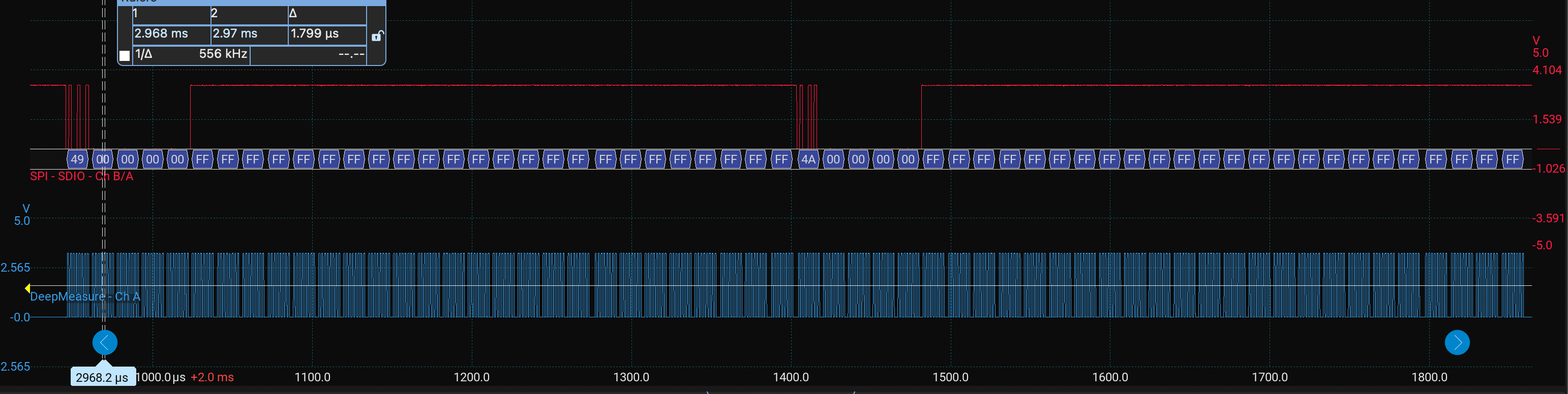
Firstly manually measuring the clock frequency shows 556 kHz, it should be closer to 562.5 kHz theoretically but we will leave that discrepancy for now. If I take a longer measurement across the whole segment it measures 558.43 kHz which is closer but not quite there.
Importantly we see the following packets:
49 00 00 00 00 FF=CMD9+ FF from chip deselect4A 00 00 00 00 FF=CMD10+ FF from chip deselect
With some large waiting gaps in between, let’s check out the MISO:
For CMD9 we have:
00 FF FE 40 0E 00 32 5B 59 00 00 E8 F7 7F 80 0A 40 00 39 7B 18 FF
This consists of the 00 R1, then FF wait byte, the FE data token, then a 16 byte register, two CRC bytes and a final dummy/wait byte which fits exactly as we would expect. Let’s break it down:
| Bytes | Meaning |
|---|---|
| 00 | R1 response: ready |
| FF | wait/dummy byte |
| FE | data token |
| 40 0E 00 32 5B 59 00 00 E8 F7 7F 80 0A 40 00 39 | CSD register, 16 bytes |
| 7B 18 | Data CRC bytes |
| FF | Finally dummy/wait byte |
We can have a go at decoding the CSD register by referring back to the SD Physical Layer Simplified Specification linked to in a previous post. It is at CSD table 5-3 and CSD v2.0 table 5-16.
Let’s say byte 0 is the first byte and byte 15 is the last (furthest right byte), some key data would be:
| Bit Field | CSD bit slice | Byte Index | Extraction | Value | Meaning |
|---|---|---|---|---|---|
| CSD_STRUCTURE | [127:126] | byte 0, bits 7:6 | csd[0] » 6 | 1 | CSD v2.0, used by SDHC/SDXC |
| TRAN_SPEED | [103:96] | byte 3 | csd[3] | 0x32 | Encoded transfer speed. |
| READ_BL_LEN | [83:80] | byte 5, bits 3:0 | csd[5] & 0x0F | 9 | max read block length = 2^9 = 512 bytes |
| C_SIZE | [69:48] | byte 7 bits 5:0, byte 8, byte 9 | ((csd[7] & 0x3F) « 16) | (csd[8] « 8) | csd[9] | 0x00E8F7 | capacity field |
| WRITE_BL_LEN | [25:22] | byte 12 bits 1:0, byte 13 bits 7:6 | ((csd[12] & 0x03) « 2) | (csd[13] » 6) | 9 | max write block length = 2^9 = 512 bytes |
Here is the code I used to extract the values:
uint8_t csd_structure = (csd[0] >> 6) & 0x03u;
uint8_t tran_speed    = csd[3];
uint8_t read_bl_len   = csd[5] & 0x0Fu;

uint32_t c_size = ((uint32_t)(csd[7] & 0x3Fu) << 16) |
                  ((uint32_t)csd[8] << 8) |
                  ((uint32_t)csd[9]);

uint8_t write_bl_len = ((csd[12] & 0x03u) << 2) |
                       ((csd[13] >> 6) & 0x03u);
Also for CSD v2.0, the capacity is calculated as (C_SIZE + 1) * 512 * 1024;. Using C_SIZE = 0x00E8F7 = 59639, the capacity is (59639 + 1) * 512 KiB = 31,268,536,320 bytes, which is about 31.27 GB or 29.12 GiB. That is consistent with a nominal 32 GB card.
For the maximum transmission speed per data line of 0x32 = 0011 0010. The spec defines bits 2:0 as the transfer rate and bits 6:3 as the time value multiplier so 2.5 * 10 Mbit/s = 25 Mbit/s. So now we know the card’s encoded maximum transfer rate per data line. It does not mean my SPI bus is currently running at 25 Mbit/s; the actual SPI clock is still set by the STM32 SPI prescaler.
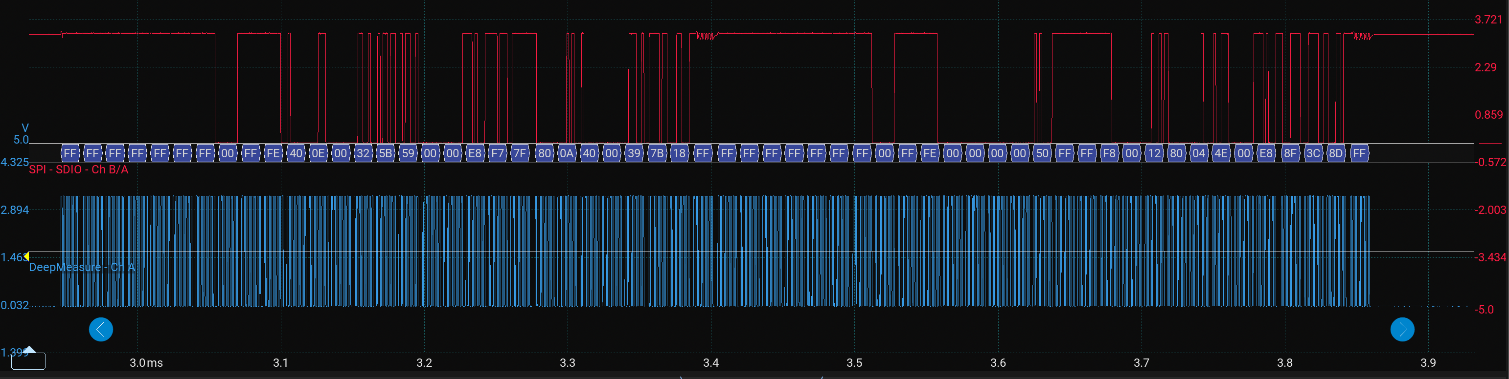
For CMD10 response we have:
00 FF FE 00 00 00 00 50 FF FF F8 00 12 80 04 4E 00 E8 8F 3C 8D FF
This is at CID table 5-2 in the sd card docs. Again, if we name the left hand byte 0 and the furthest right hand byte 15 we can map out some key bit fields on the CID register:
| Field | CID bit slice | Byte Index. | Value | Meaning |
|---|---|---|---|---|
MID |
[127:120] |
byte 0 | 0x00 |
Manufacturer ID |
OID |
[119:104] |
bytes 1–2 | 0x0000 |
OEM/Application ID |
PNM |
[103:64] |
bytes 3–7 | 00 50 FF FF F8 |
Product name, not clean ASCII here |
PRV |
[63:56] |
byte 8 | 0x00 |
Product revision 0.0 |
PSN |
[55:24] |
bytes 9–12 | 0x1280044E |
Product serial number |
| reserved | [23:20] |
byte 13 bits 7:4 | 0x0 |
Reserved |
MDT |
[19:8] |
byte 13 bits 3:0 + byte 14 | 0x0E8 |
Manufacturing date |
CRC |
[7:1] |
byte 15 bits 7:1 | 0x47 |
CID internal CRC7 |
| end bit | [0:0] |
byte 15 bit 0 | 1 |
Always 1 |
Here is the extraction code:
uint8_t mid = cid[0];

uint16_t oid = ((uint16_t)cid[1] << 8) |
               ((uint16_t)cid[2]);

char pnm[6];
pnm[0] = (char)cid[3];
pnm[1] = (char)cid[4];
pnm[2] = (char)cid[5];
pnm[3] = (char)cid[6];
pnm[4] = (char)cid[7];
pnm[5] = '\0';

uint8_t prv_major = (cid[8] >> 4) & 0x0Fu;
uint8_t prv_minor = cid[8] & 0x0Fu;

uint32_t psn = ((uint32_t)cid[9] << 24) |
               ((uint32_t)cid[10] << 16) |
               ((uint32_t)cid[11] << 8) |
               ((uint32_t)cid[12]);

uint16_t mdt = ((uint16_t)(cid[13] & 0x0Fu) << 8) |
               ((uint16_t)cid[14]);

uint16_t year = 2000u + ((mdt >> 4) & 0xFFu);
uint8_t month = mdt & 0x0Fu;

uint8_t cid_crc7 = (cid[15] >> 1) & 0x7Fu;
uint8_t end_bit = cid[15] & 0x01u;
There is not much here that we can really make use of other than the serial number for the card, and the manufacturing date: The CID manufacturing date field is 0x0E8. The upper 8 bits give the year offset from 2000, and the lower 4 bits give the month. That gives year 2000 + 14 = 2014 and month 8, so the card reports August 2014.
The CID register reports a manufacturing date of August 2014, which is odd because this card was bought recently. The other CID fields also do not decode into a clean manufacturer/product string, so I’m curious as to what that might mean. CMD10 returned a valid looking 16 byte payload after the expected data token which is great. For those interested I’m now going to investigate the card capacity further due to the strange results from CMD10.
Investigating my microSD card further
Well first things first I plug the microSD card into the laptop to find an empty DCIM folder on there which is not a good start as this is a fresh card from the pack.
Here are some pictures of my card which is a SanDisk Ultra 32GB microSD:
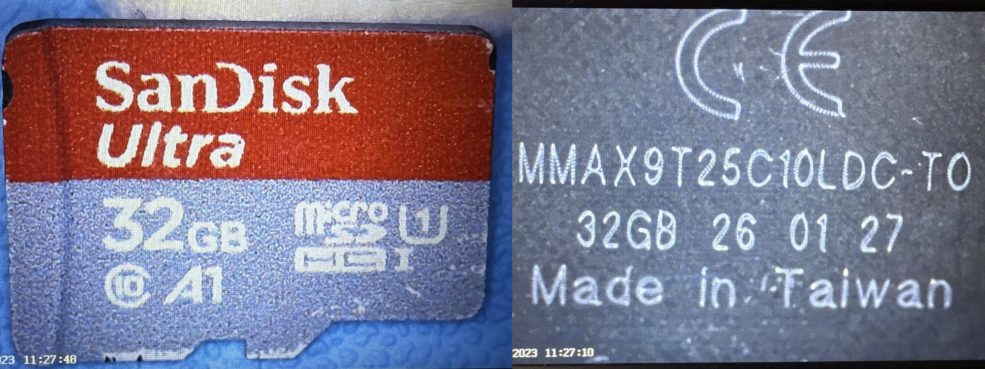
For a SanDisk Ultra I can find a few typical CID values online which do not agree with the ones I have read: MID: 0x03 OID: 0x5344, which is ASCII for “SD” PNM: Often something like SDxxx, SUxxG or SCxxG
Furthermore the markings on the back look like a fairly modern production marking, which doesn’t really align with the 2014 reported manufacturing date! I found some online discussions suggesting that back side markings can differ between genuine and counterfeit cards, but I do not want to rely on that alone. The mismatch between the SanDisk label and the odd CID fields, plus the full capacity and speed test results are curious.
I have installed F3 Write 10.0 with homebrew, there are equivalents for Windows such as H2testw and linux too. This will access the card, and try to write files to fill the reported capacity to test how close it actually is. This is due to many fakes being found that may be a much lower capacity card reporting at a higher capacity. I’ve plugged the card in and run f3write /Volumes/SUSMICROSD/.
F3 reports the free space at about 29.06 GB. That is close to the CSD derived 29.12 GiB once formatting overhead and decimal/binary unit differences are considered, so the capacity itself does not look fake from this test. The average F3 write speed was around 8.69 MB/s, which is below the labelled Class 10 expectation. That is another suspicious sign, although I should be careful here because the result can depend on the reader, USB hub, filesystem, write pattern, and test setup.
Here is a plot of the write speeds per 1GB file:
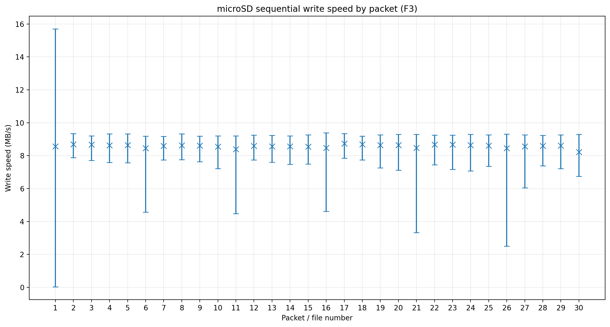
To be fair the write speed is very consistent, although every fifth file seems to have a lower speed bound.
The writes are complete so we’ll run f3read /Volumes/SUSMICROSD/ to see how well it will read the files back, there should be no corruptions here. Hmm it is starting to look suspicious again, I would expect the F3 read speeds to be much higher given the classification but currently I’m seeing 20 MB/s average speeds.
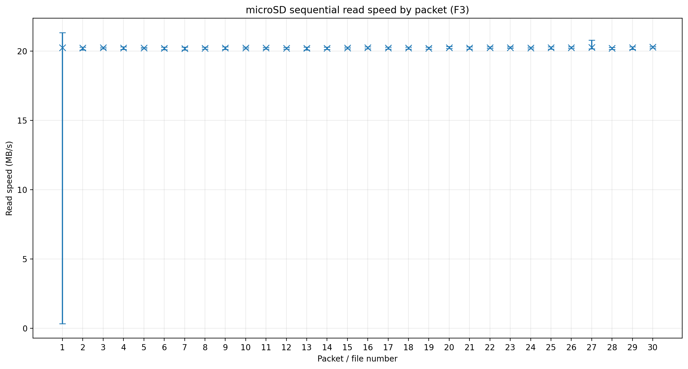
I expected a SanDisk Ultra card to read faster than this, but the full F3 read passed without corruption, so this looks more like a suspicious/performance concern than a fake capacity result. The CID and performance are suspicious enough that I would not use it as a trusted reference card, but it is fine for my purposes for SPI logging at the moment.
That concludes the post for today, next I’ll tackle reading and writing raw blocks.
Copyright © 2026 David O’Connor