STM32 #12: Talking to a microSD card over SPI
In the previous two posts I looked at why I want removable local storage on the STM32F103x, then built a small SPI1 board support package using libopencm3. The full storage stack I’m working towards looks like this:
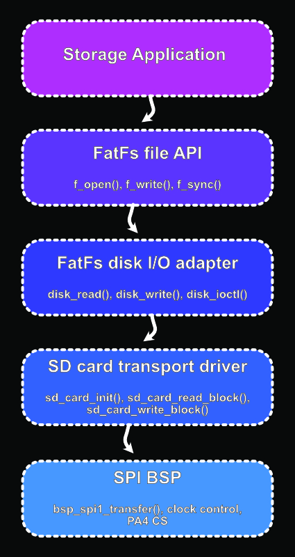
This post focuses on the SD card transport layer. The goal is to talk to the card at the block level using the bsp_spi.h API so that I can read and write raw 512 byte sectors before messing with FatFs, because it will have no knowledge of how the micro is wired to the microSD card. That will happen through the disk I/O adapter layer between FatFs and SD Card transport. So the sd card driver will expose very basic functions such as:
sd_status_t sd_card_init(void);
sd_status_t sd_card_read_block(uint32_t block, uint8_t *buffer);
sd_status_t sd_card_write_block(uint32_t block, const uint8_t *buffer);
Once we confirm these functions working the FatFs implementation should be a little less difficult to figure out and debug.
A note on the SPI BSP developed in the last post
In the last post I kept the SPI bsp deliberately small to understand what the core concepts were and to make it easy to follow. I have since spent many hours digging deeper into it making the package a little more defensive. I’ve summarised the main changes here, which I may cover in the future:
- SPI transfers now return a status instead of assuming things worked out okay
- Wait loops now have timeout limits
- Basic STM32 SPI errors such as overrun and mode fault are checked
- Buffer functions validate their parameters
- the baud rate is only changed once the SPI peripheral is not busy
The extra robustness is fairly important because an SD card is a removable piece of hardware. So it may not respond, it may be absent, the wiring may be wrong (holds breath), or the card might be busy internally. I didn’t want the final data logger to be sitting forever in a while loop.
The SD card layer does not call those low level wait helpers directly. It only sees the public SPI BSP API. Internally, though, the SPI BSP now uses timeout based waits so that calls like bsp_spi1_transfer() and bsp_spi1_write_buffer() can fail cleanly instead of blocking forever.
What actually is SD over SPI?
When an SD card powers up, by default it boots into its native “SD mode” which is very fast but uses quite a few connections to make it happen as explained in the last post. To use it over SPI, the host has to send a reset command while chip select is asserted in the correct way.
Once the card is in the SPI mode, commands and data are exchanged as normal SPI bytes. The STM32 is the controller (master), and the microSD card is the peripheral (slave), and every byte sent by the STM32 also clocks one byte back from the SD card. This is why in the SPI BSP we added the transfer function rather than only separate read and write:
bsp_spi_status_t bsp_spi1_transfer(uint8_t tx_data, uint8_t *rx_data);
Even if we only care about reading data, we still have to transmit dummy bytes, usually 0xFF, to generate clock pulses.
SD Card initialisation sequence
The initialisation sequence for SPI is this:
- Power on
- Keep CS (chip select) high
- Send at least 74 dummy clock pulses
- Pull CS low
- Send CMD0 to access idle state
- Send CMD8 to check the voltage range and card version
- Repeatedly send CMD55 + ACMD41 until the card leaves idle state (R1=0x00)
- Detect whether the card is SDHC/SDXC or SDSC
- Increase the SPI speed
So the first goal for developing this driver will be to reset the card, ID it, and get it out of the idle state.
SD commands are six byte packets
In SPI mode, most SD commands are sent as six bytes:
[Command] [arg3] [arg2] [arg1] [arg0] [CRC]
The command byte includes the command index. For example CMD0 is sent as command index 0 with the required start/transmission bits added. The argument is a 32-bit value split into four bytes. The CRC byte is ignored in SPI mode after initialisation, but CMD0 and CMD8 still need to have valid CRC values during the initialisation.
Here is a good summary of the command/response registers from a nintendo hardware hacking site of all places. On this page there is a index with great coverage for the SD protocol.
Waiting for a response
SD cards are a little different to most other SPI peripherals because the response does not necessarily appear immediately. After sending a command the card might return 0xFF for several bytes before finally returning a useful response. So the driver needs a helper function that keeps clocking the bus and waiting for either a valid response, or a timeout to be hit. This is why the timeout additions in the SPI BSP become quite important. The SD card layer should not have to assume the card will always respond.
SD command responses in SPI mode
There are 3 main response types that will appear during initialisation
| Response | Size in SPI mode | Used by | Meaning |
|---|---|---|---|
| R1 | 1 byte | CMD0, CMD55, ACMD41, CMD17, CMD24 | Main status response. Each bit is a flag. |
| R3 | 5 bytes | CMD58 | R1 byte followed by 4 OCR bytes. |
| R7 | 5 bytes | CMD8 | R1 byte followed by 4 bytes echoing voltage/check-pattern information. |
Both R3 and R7 start with a R1 byte, so the driver can wait for the R1 response and then read the extra four bytes if the command expects them.
R1 response byte
During initialisation the SD card mostly returns an R1 response. This is a single status byte where each bit is a flag.
A response of 0x00 means no error flags are set and the card is ready. During initialisation, 0x01 is also expected because bit 0 means the card is still in idle state:
| Bit | Mask | Meaning |
|---|---|---|
| 7 | 0x80 |
Always 0 in a valid R1 response |
| 6 | 0x40 |
Parameter error |
| 5 | 0x20 |
Address error |
| 4 | 0x10 |
Erase sequence error |
| 3 | 0x08 |
CRC error |
| 2 | 0x04 |
Illegal command |
| 1 | 0x02 |
Erase reset |
| 0 | 0x01 |
In idle state |
Some examples of the R1 responses:
0x01 = 0000 0001 = valid R1, card is idle
0x00 = 0000 0000 = valid R1, ready/no error
0x05 = 0000 0101 = valid R1, idle + illegal command
0xFF = 1111 1111 = not a valid R1 response, bit 7 is 1, keep waiting
The important… bit… is that R1 is a bit field. More than one flag can be set at once. So 0x05 is just:
0x05 = 0x04 | 0x01
Which is a valid R1 format response, but reports idle + illegal command
Bit 7 is different from the others. In a valid R1 response it should always be zero. That is useful because while the SD card is not ready to respond, it will often keep returning 0xFF. Therefore the driver can keep clocking the bus until it receives a byte where bit 7 has cleared.
CMD0: Reset the card into SPI mode
CMD0 is the reset command, it’s also the command that should put the card into SPI mode if following the initialisation sequence mentioned earlier. If that is done the expected response should be R1 = 0x01 meaning the card is in idle state.
CMD8: Check voltage range and card version
CMD8 is used to check whether the card supports the expected voltage range and to help differentiate between the newer SD v2 cards and the older ones. For a modern SDHC card, we should expect CMD8 to return a R7 response which contains the voltage pattern that was sent in the command argument. This is important to differentiate between older SDSC and newer SDHC/SDXC cards.
The common argument is 0x000001AA and the expected echoed check pattern should be 0xAA.
ACMD41: Wait for the card to finish initialising
ACMD41 is an application specific command, so it has to be preceded by CMD55. The sequence should look like this:
- CMD55
- ACMD41
- Check response
- Repeat until response is 0x00 or timeout
- Card should leave idle state
If a timeout error happens here then something is wrong with the setup like no card, bad wiring, incorrect power, or a bad command sequence.
For SD v2 cards (e.g. SDHC and SDXC), the High Capacity Support (HCS) bit can be set in the argument: ACMD41 argument = 0x40000000.
CMD58: Read OCR and detect SDHC
After the card has initialised, CMD58 reads the SD cards Operating Conditions Register (OCR) which is a 32 bit register containing the cards Vdd voltage profile and init status. This should return an R3 response which contains an R1 response followed by the 4 byte OCR contents. Here is the bit flag table, ONLY for over SPI, the SDMMC table is different, here is the bit field of the SPI response:
| R3 response bits | Meaning |
|---|---|
| 39:32 | R1 response byte |
| 31:0 | OCR register |
OCR Register:
| Bit | Flag | 0 | 1 |
|---|---|---|---|
| 31 | Power up status | Busy | Ready |
| 30 | Capacity (CCS) | SDSC | SDHC or SDXC |
| 29 | UHS-II support | no | yes |
| 28:25 | Reserved | ||
| 24 | Switching to 1.8v accepted (UHS-I) | no | yes |
| 23 | VDD Operating Voltage 3.5 - 3.6 supported | no | yes |
| 22 | VDD Operating Voltage 3.4 - 3.5 supported | no | yes |
| 21 | VDD Operating Voltage 3.3 - 3.4 supported | no | yes |
| 20 | VDD Operating Voltage 3.2 - 3.3 supported | no | yes |
| 19 | VDD Operating Voltage 3.1 - 3.2 supported | no | yes |
| 18 | VDD Operating Voltage 3.0 - 3.1 supported | no | yes |
| 17 | VDD Operating Voltage 2.9 - 3.0 supported | no | yes |
| 16 | VDD Operating Voltage 2.8 - 2.9 supported | no | yes |
| 15 | VDD Operating Voltage 2.7 - 2.8 supported | no | yes |
| 14:0 | Reserved |
The CCS bit is important because it tells us whether the card uses block addressing. For SDHC/SDXC cards, reads and writes use 512 byte block numbers directly. For older SDSC cards, the command argument is a byte address.
Block addressing
For the SDHC and SDXC cards, the address passed to CMD17 or CMD24 is a block number. For the older SDSC cards, the address is a byte address.
So for SDHC:
address = block_number;
For SDSC:
address = block_number * 512;
For this application I’m using an SDHC microSD card but the driver should still know which type of card it has initialised.
CMD17: reading a 512 byte block
Once initialisation is good, the next step is to read a single raw block. The single block read command is CMD17. The sequence for this is:
- Send CMD17 with block address
- Wait for R1 response 0x00
- Wait for a data token 0xFE
- Read 512 bytes
- Read and discard 2 CRC bytes
- Release CS
- Send an extra dummy byte
At this point we’re still below FatFS, just asking the card for a numbered 512 byte sector. I will leave this to the next post, as this one is getting big.
CMD24: Writing a 512 byte block
This command writes a single block, here is the sequence:
- Send CMD24 with block address
- Wait for R1 response 0x00
- Send data token 0xFE
- Send 512 bytes
- Send 2 dummy CRC bytes
- Read data response token
- Wait while the card is busy
- Release CS
- Send one extra dummy byte
Write handling needs much more care than reading because the card could remain busy internally after the command/data is accepted. This will also be left to the next post.
The CRC byte
In an SPI mode driver, CRC checking is usually not used after the initial startup commands, so dummy CRC bytes such as 0xFF are commonly sent. CMD0 and CMD8 are startup exceptions:
| Command | CRC |
|---|---|
| CMD0 | 0x95 |
| CMD8 | 0x87 |
This is explained on ChaNs website in the links posted in the previous post.
Summary of the commands
| Command | Sent byte | Argument | CRC byte | Response | Used for |
|---|---|---|---|---|---|
| CMD0 | 0x40 |
0x00000000 |
0x95 |
R1 | Reset card and enter idle/SPI mode |
| CMD8 | 0x48 |
0x000001AA |
0x87 |
R7 | Check SD v2 support and voltage range |
| CMD55 | 0x77 |
0x00000000 |
0xFF |
R1 | Prefix before application-specific command |
| ACMD41 | 0x69 |
0x40000000 |
0xFF |
R1 | Application specific, Initialise card, with HCS bit set |
| CMD58 | 0x7A |
0x00000000 |
0xFF |
R3 | Read OCR and detect SDHC/SDXC |
| CMD17 | 0x51 |
block address | 0xFF |
R1 + data token | Read one 512-byte block |
| CMD24 | 0x58 |
block address | 0xFF |
R1 + data response | Write one 512-byte block |
First implementation: send commands, read responses
Before getting into full block read and writes, let’s build the smallest useful part of the SD card transport layer, which will consist of sending a command and reading the response.
From the previous post the SPI BSP has its own status enum because it knows about the STM32 SPI level issues:
typedef enum {
    BSP_SPI_OK = 0,
    BSP_SPI_ERR_TIMEOUT,
    BSP_SPI_ERR_OVERRUN,
    BSP_SPI_ERR_MODE_FAULT,
    BSP_SPI_ERR_PARAM,
} bsp_spi_status_t;
The SD card transport layer will have its own status enum because it should report SD card level errors too:
typedef enum {
    SD_OK = 0,
    SD_ERR_SPI,
    SD_ERR_TIMEOUT,
    SD_ERR_PARAM,
    SD_ERR_BAD_RESPONSE,
    SD_ERR_UNSUPPORTED_CARD,
} sd_status_t;
You could make a mapping to translate the bsp_spi1 errors through the sd_card layer but I’m going to leave it for this post.
The SD driver does not need to expose all the SPI STM32 detail to the layers above. If the SPI transfer fails, the SD layer can initially report SD_ERR_SPI. The error status can be quite helpful when debugging over UART.
Once CS has been pulled low, every exit path should release the card again. Both the success and error paths need to leave the SPI bus in the same state: CS high, followed by one extra dummy byte to provide clocks after deselection, so I’m creating a helper to keep the code clean called sd_deselect() and whilst I’m at it let’s create a wrapper for making the CS pin low to make the naming more consistent:
#include "bsp_spi.h" // from the last post

static void sd_select(void) {
    bsp_spi1_cs_low();
}

static void sd_deselect(void) {
    bsp_spi1_cs_high();
    // Provide 8 extra clocks after deselecting the card.
    (void)bsp_spi1_transfer(0xFFu, NULL);
}
On to writing the dummy bytes needed to set the card into SPI mode…
static sd_status_t sd_clock_dummy_bytes(size_t count) {
    for (size_t i=0; i<count; ++i) {
        bsp_spi_status_t spi_status = bsp_spi1_transfer(0xFFu, NULL);

        if (spi_status != BSP_SPI_OK) { return SD_ERR_SPI; }
    }

    return SD_OK;
}
The next helper will wait for an R1 response, because the card may return 0xFF for a while before it gives a useful response. This function will keep clocking the bus until the top bit clears or a timeout is reached.
#define SD_RESPONSE_TIMEOUT 100u

static sd_status_t sd_wait_r1(uint8_t *r1) {
    if (r1 == NULL) { return SD_ERR_PARAM; }

    for (uint32_t i=0; i<SD_RESPONSE_TIMEOUT; ++i) {
        uint8_t response = 0xFFu;

        bsp_spi_status_t spi_status = bsp_spi1_transfer(0xFFu, &response);
        if (spi_status != BSP_SPI_OK) { return SD_ERR_SPI; }

        // Check for valid R1 response = bit 7 is always 0.
        if ((response & 0x80u) == 0u) {
            *r1 = response;
            return SD_OK;
        }
    }

    return SD_ERR_TIMEOUT;
}
To reiterate, the reason for checking 0x80 is that bit 7 is always zero in a valid R1 response. While the card is not ready it will usually keep returning 0xFF, where bit 7 is still set. So the helper clocks the bus until it sees a byte where bit 7 has cleared.
We are going to add a helper function that will read the response_tail bytes that follow the R1 response for CMD8
static sd_status_t sd_read_bytes(uint8_t *buffer, size_t len) {
    if ((buffer == NULL) && (len != 0u)) {return SD_ERR_PARAM;}

    bsp_spi_status_t spi_status = bsp_spi1_read_buffer(buffer, len);
    if (spi_status != BSP_SPI_OK) {return SD_ERR_SPI;}

    return SD_OK;
}
Now the command helper coming up has the tools to send the standard six byte SD command packet and read the response
The first byte of the command packet contains the command index in the format: 01xxxxxx, where the lower six bits contain the command index. We will do this by using 0x40 which is binary 0100 0000 then bitwise OR the cmd inserts it into the lower 6 bits. E.g. for CMD8:
0x40 | 8 = 0x48 // CMD8
I’ve also added some protection into converting the command, all commands must be 6 bit so we can control that to prevent a bad cmd parameter from altering the upper bits with cmd & 0x3Fu. This works by always ensuring the upper bits of the command are zeroed out as 0x3Fu = 0011 1111 then when this is bitwise OR by 0x40u the correct upper bits will always be set.
The argument bytes are isolated from the full 32 bit sequence by shifting the relevant bits to the right and casting to a uint8_t which keeps only the lowest 8 bits.
The command helper takes a pointer for the first R1 response byte. It also takes an optional response_tail buffer for commands such as CMD8 and CMD58, where the R1 byte is followed by four more bytes.
static sd_status_t sd_send_command(uint8_t cmd,
                                   uint32_t arg,
                                   uint8_t crc,
                                   uint8_t *r1,
                                   uint8_t *response_tail,
                                   size_t response_tail_len) {

    // Parameter error checking
    if (r1 == NULL) { return SD_ERR_PARAM; }
    if ((response_tail == NULL) && (response_tail_len != 0u)) {
        return SD_ERR_PARAM;
    }

    // CMD packet:
    uint8_t packet[6];
    packet[0] = 0x40u | (cmd & 0x3Fu);

    // Argument bytes, most significant byte first
    // Casting isolates the lowest 8 bits:
    packet[1] = (uint8_t)(arg >> 24);
    packet[2] = (uint8_t)(arg >> 16);
    packet[3] = (uint8_t)(arg >> 8);
    packet[4] = (uint8_t)(arg);
    packet[5] = crc;

    // CS pin low
    sd_select();

    // Write to the buffer
    bsp_spi_status_t spi_status = bsp_spi1_write_buffer(packet, sizeof(packet));
    if (spi_status != BSP_SPI_OK) {
        sd_deselect();
        return SD_ERR_SPI;
    }

    // Wait for r1 response
    sd_status_t status = sd_wait_r1(r1);
    if (status != SD_OK) {
        sd_deselect();
        return status;
    }

    // Check if response contains more than just r1 and read
    if (response_tail_len != 0u) {
        status = sd_read_bytes(response_tail, response_tail_len);
        if (status != SD_OK) {
            sd_deselect();
            return status;
        }
    }

    sd_deselect();

    return SD_OK;
}
For the first test I’m not going to fully initialise the card, but start the process just to prove that the card can enter SPI mode and respond to CMD0/CMD8, so let’s give the first pass of sd_card_init() a go:
sd_status_t sd_card_init(void) {
    uint8_t r1 = 0xFFu;

    // Set transfer speed
    bsp_spi_status_t spi_status = bsp_spi1_set_slow();
    if (spi_status != BSP_SPI_OK) { return SD_ERR_SPI; }

    // SD cards need at least 74 clock pulses with CS high before CMD0
    // 1 SPI byte transfer produces 8 clock pulses, so 10 dummy bytes gives 80 clock pulses
    bsp_spi1_cs_high();
    sd_status_t status = sd_clock_dummy_bytes(10);
    if (status != SD_OK) { return status; }

    // CMD0: Reset card, enter idle state
    status = sd_send_command(0, 0x00000000u, 0x95u, &r1, NULL, 0u);
    if (status != SD_OK) { return status; }
    if (r1 != 0x01u) { return SD_ERR_BAD_RESPONSE; }

    // CMD8: Check voltage range and SD v2 support
    uint8_t r7_tail[4];
    status = sd_send_command(8,
                             0x000001AAu,
                             0x87u,
                             &r1,
                             r7_tail,
                             sizeof(r7_tail));
    if (status != SD_OK) { return status; }

    // For a modern SDHC card, CMD8 should be accepted while still idle.
    if (r1 != 0x01u) { return SD_ERR_BAD_RESPONSE; }

    // Expected R7 tail for CMD8 argument 0x000001AA:
    // r7_tail[0] = 0x00
    // r7_tail[1] = 0x00
    // r7_tail[2] = 0x01
    // r7_tail[3] = 0xAA
    if ((r7_tail[2] != 0x01u) || (r7_tail[3] != 0xAAu)) {
        return SD_ERR_BAD_RESPONSE;
    }

    return SD_OK;
}
Testing
Check out the earlier post about microSD and wiring to an STM32f103x for SPI if you missed that.
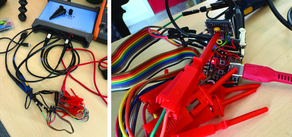
If you have a UART module written, you can use that to report the response values back to a terminal connected to the STM32F1xx. However, for fun, and in case you do not have UART debug output written yet, you can also inspect the SPI lines directly with a 2-channel oscilloscope with logic analyser features.
Since I only have two channels available, I am doing this as two separate captures:
- SCK + MOSI, to check what the STM32 sends
- SCK + MISO, to check what the SD card returns
For this smoke test, CMD0 should return 0x01 and CMD8 should return 0x01 followed by 00 00 01 AA.
It looks like a lot, but that is because my contacts are on a ribbon cable, I’m only using two of them with the probes stuffed in the other end, which is rough and ready, but will work for this test:
Scope: SCK + MOSI
The STM32F103x should be sending:
CMD0: 40 00 00 00 00 95
CMD8: 48 00 00 01 AA 87
Let’s take a look: The blue trace is the clock signal needed for the logic analyser, and the red trace is the MOSI line (which has a 10k pull up on it):
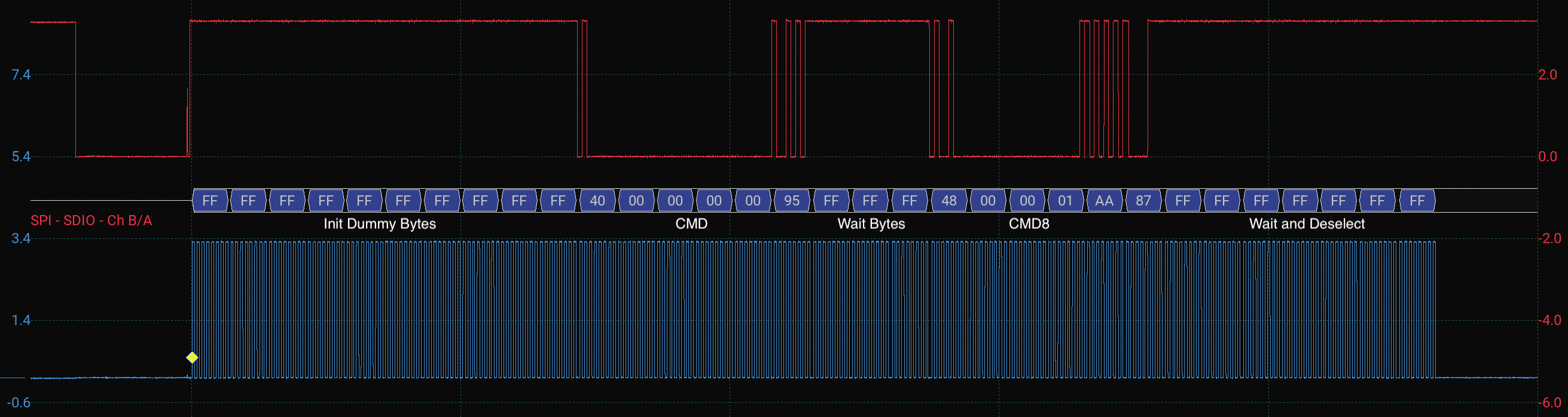
As you can see, the STM32 sends the 10 dummy bytes of 0xFF first. That gives the SD card 80 clock pulses with CS high before CMD0.
Then the STM32 sends:
CMD0: 40 00 00 00 00 95
After that there are a few 0xFF bytes while the driver clocks the bus and waits for the card response, followed by the dummy byte sent after deselecting the card.
Then the STM32 sends:
CMD8: 48 00 00 01 AA 87
After CMD8, the driver again sends dummy 0xFF bytes while waiting for the R1 response, reading the R7 response tail, and finally deselecting the card.
Scope: SCK + MISO
I’ve now hooked up the second probe to the MISO line, reset the device and captured the init sequence again. The SD card should be responding with:
CMD0 response: 01
CMD8 response: 01 00 00 01 AA
Let’s take a look on the scope. The blue trace is the clock signal again, and the red trace is now connected to the MISO line:
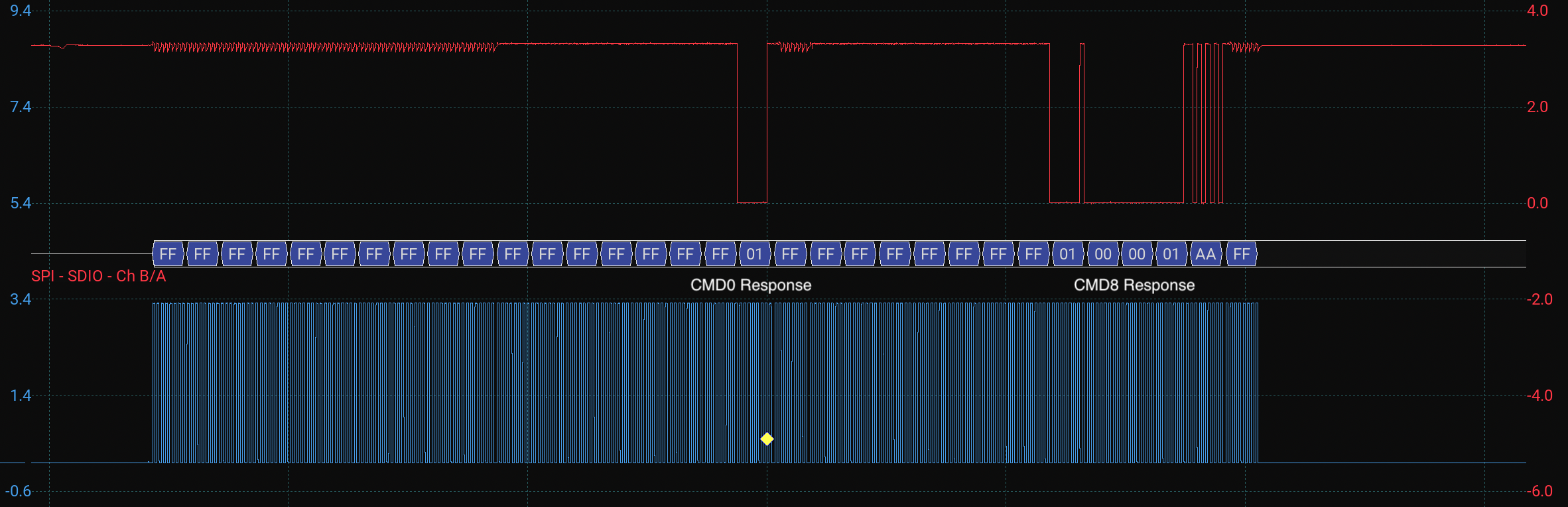
Wow it is responding!
At the start, the card returns 0xFF while the STM32 sends the initial dummy clocks and the CMD0 packet. Then the card returns: 01. That is the expected CMD0 response, meaning the card is now in idle state.
The card then returns more 0xFF bytes while the STM32 sends the CMD8 packet and clocks the bus. Finally, the card returns: 01 00 00 01 AA. This is exactly what I wanted to see. The first byte, 0x01, is the R1 response showing that the card is still in idle state. The remaining four bytes are the R7 response tail from CMD8, and the final 0xAA confirms that the check pattern was echoed back correctly.
So at this stage the card is not fully initialised yet, but the SPI wiring, command packet format, dummy clocking, R1 response handling, and CMD8 R7 response read are all working.
Next we will take a look at finishing the init sequence, then reading and writing memory blocks!
Copyright © 2026 David O’Connor